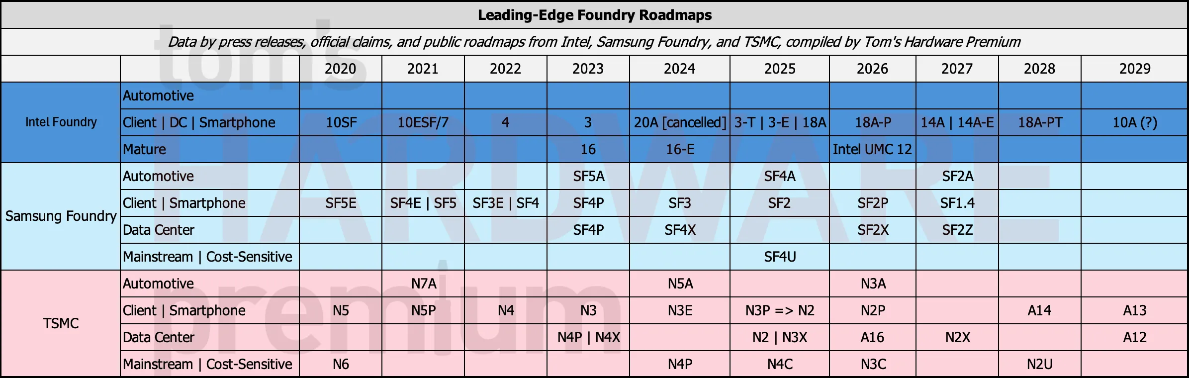
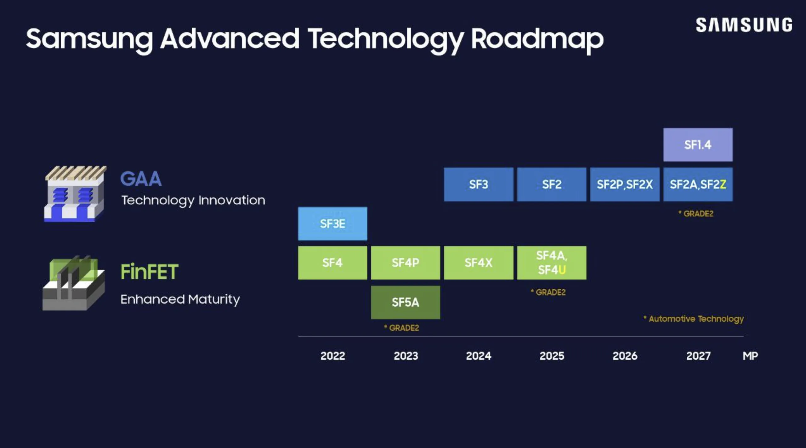
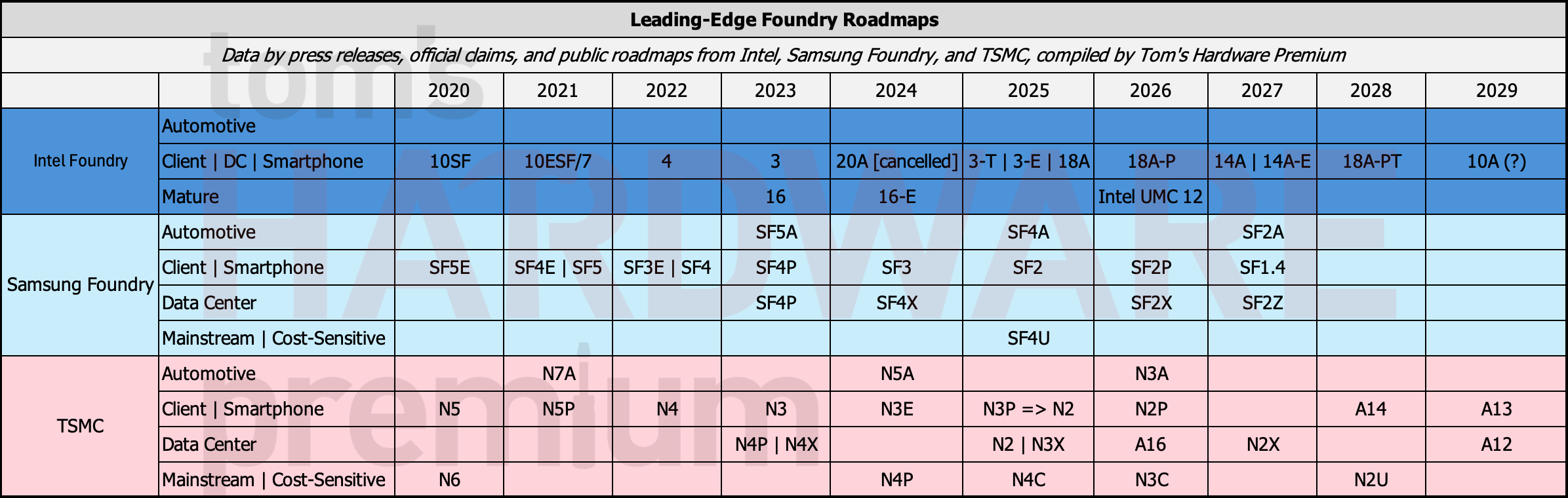
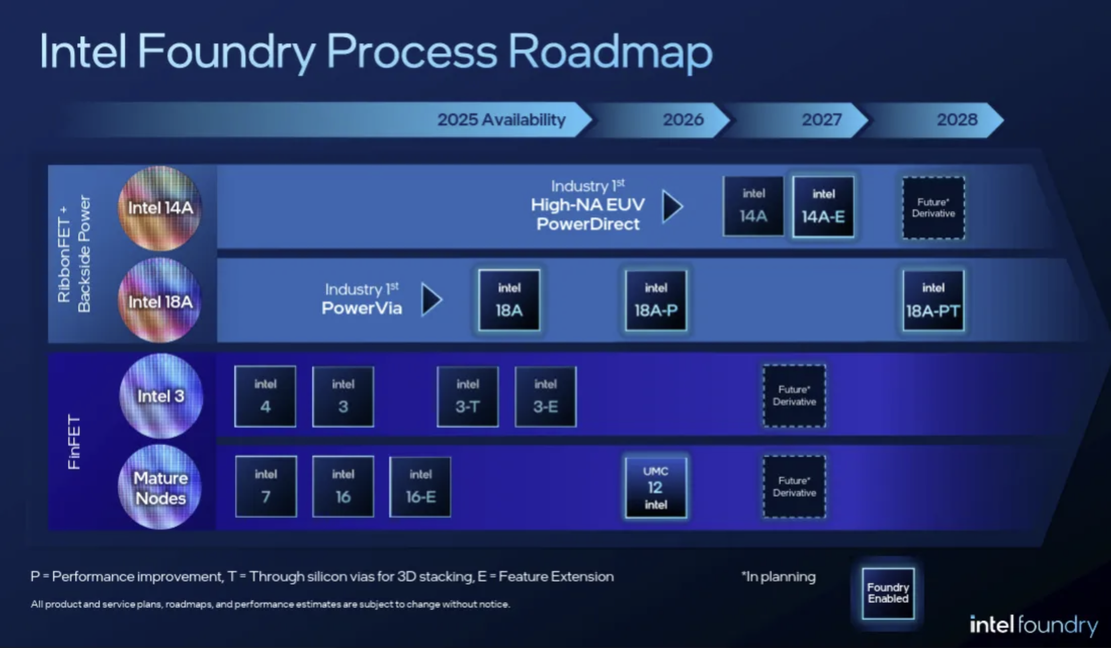
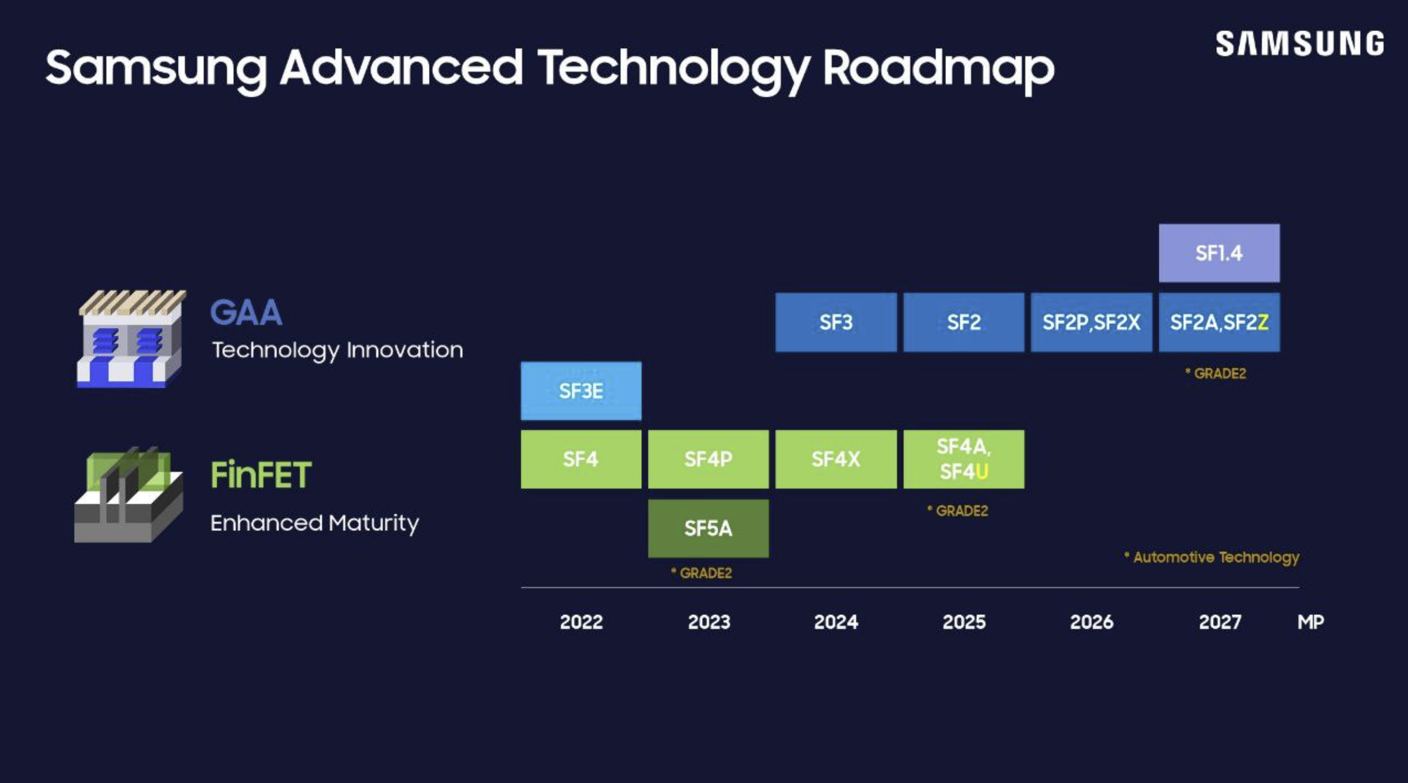
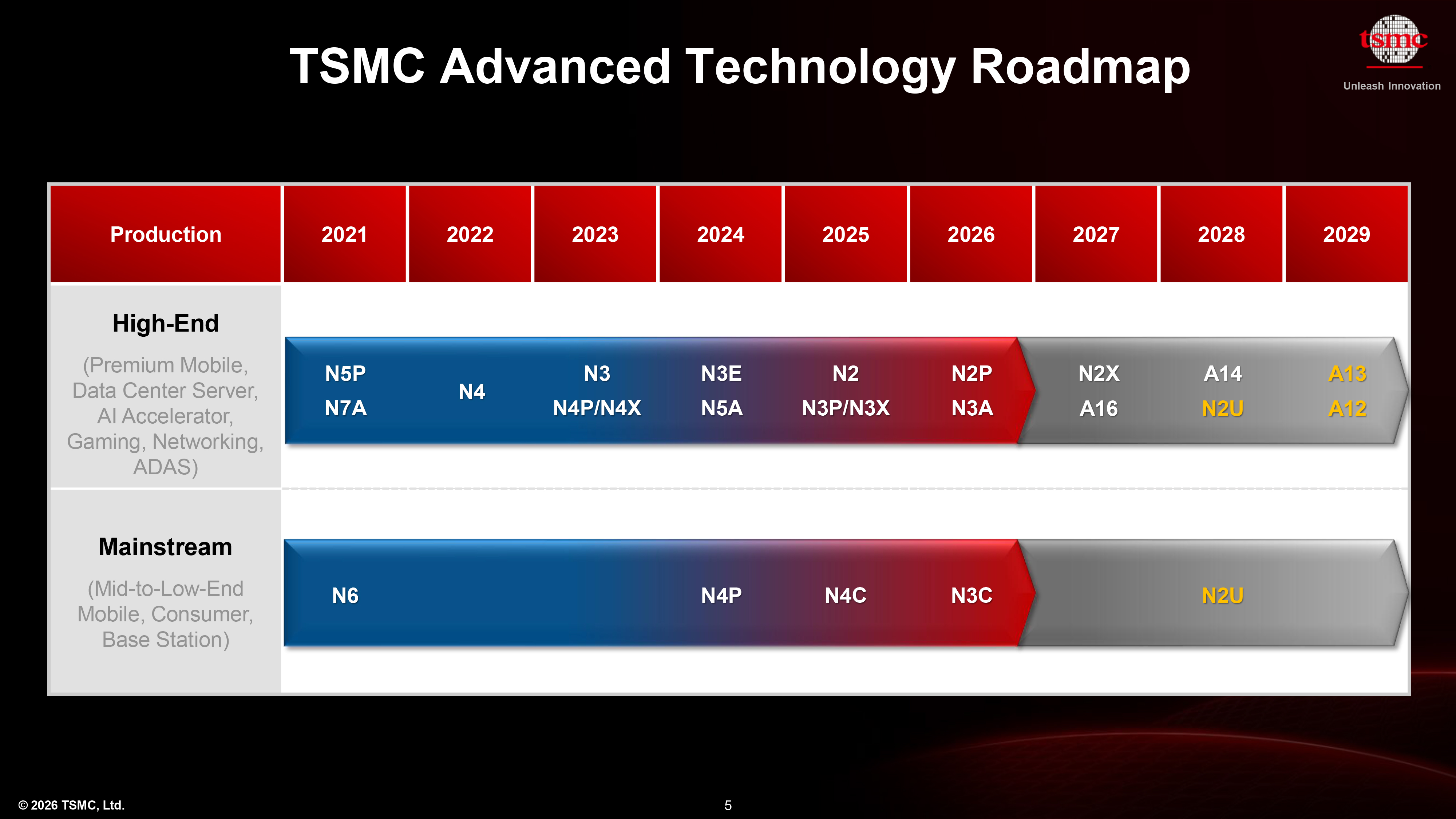
(Image credit: Getty Images / Bloomberg) All three leading-edge foundries — Intel Foundry, Samsung Foundry, and TSMC — have initiated mass production of chips using 2nm-class process technology. Samsung was the first one to start production using its SF2 node (though it could be argued that this is a rebadged SF3P ) around mid-2025, Intel followed suit with its 18A node in November (albeit at development lines in Oregon, not production lines in Arizona), and TSMC initiated high-volume manufacturing using its N2 process at two volume fabs in Taiwan in December . We outline what's next for these three leading-edge foundries. The current state of the market (Image credit: Tom's Hardware) TSMC is focused on predictable scaling, combined with aggressive specialization, which is why its roadmap is split into high-performance computing-oriented technologies with backside power delivery network (BSPDN) and cost/density-optimized nodes without it.…