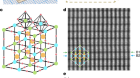
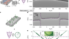
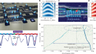
NEWS AND VIEWS 13 May 2026 An electron-beam technique that can precisely create thousands of atomic defects in a crystal could be used to build quantum devices. By Toma Susi Toma Susi is in the Faculty of Physics, University of Vienna, Vienna 1090, Austria. In 1959, the physicist Richard Feynman posed the question: “What would happen if we could arrange the atoms one by one the way we want them?” 1 This vision represents the ultimate limit of both materials science and nanotechnology — the study and control of matter down to the atomic scale. Highly focused electron beams can be used to manipulate single atoms in a crystal, but so far it has only been possible to make a handful of rearrangements at a time. Now, writing in Nature , Klein et al. 2 report a method for manipulating thousands of lattice sites in a crystal in minutes using an electron beam, creating controllable patterns of defects that promise to have intriguing quantum properties.…