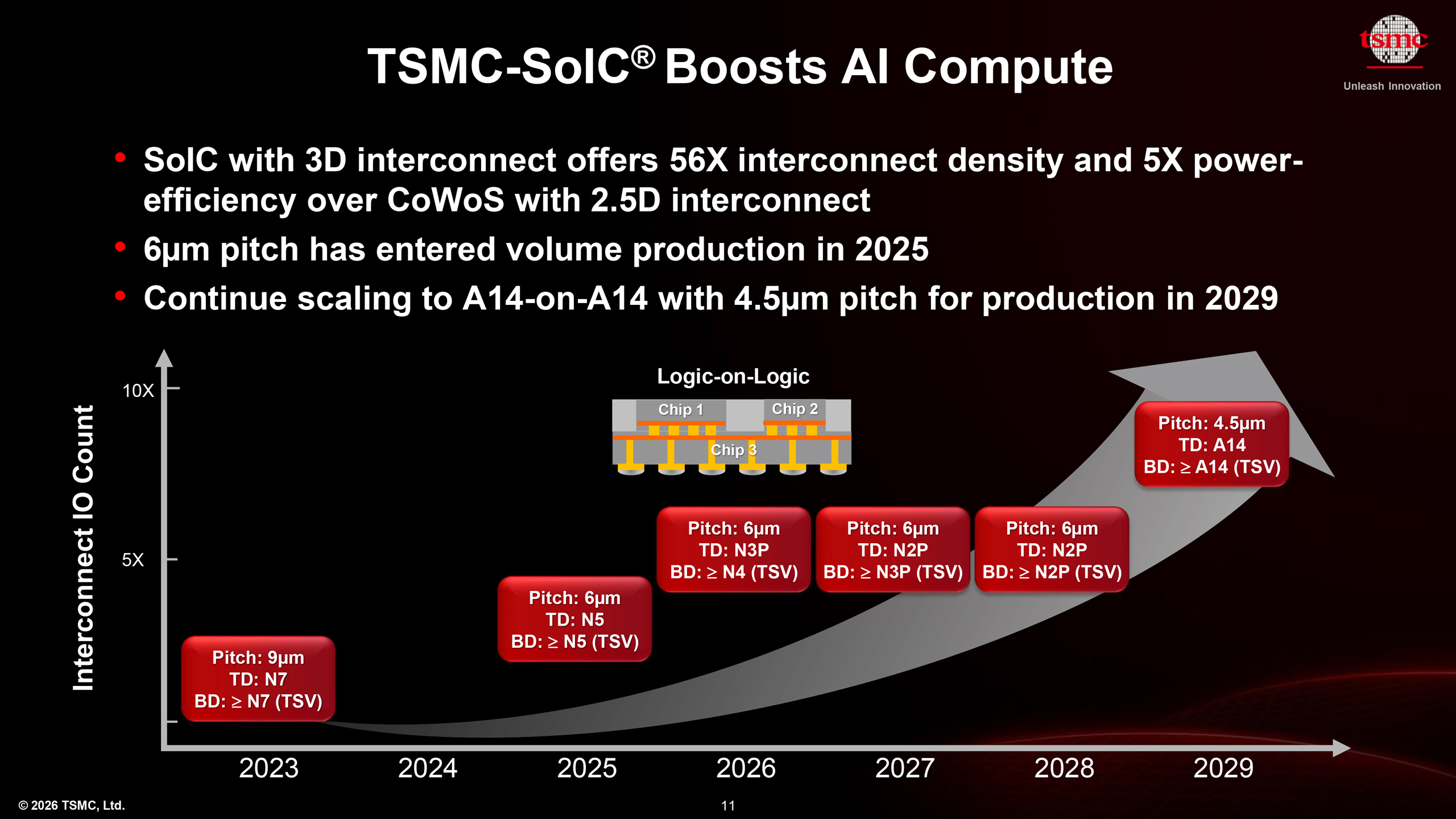
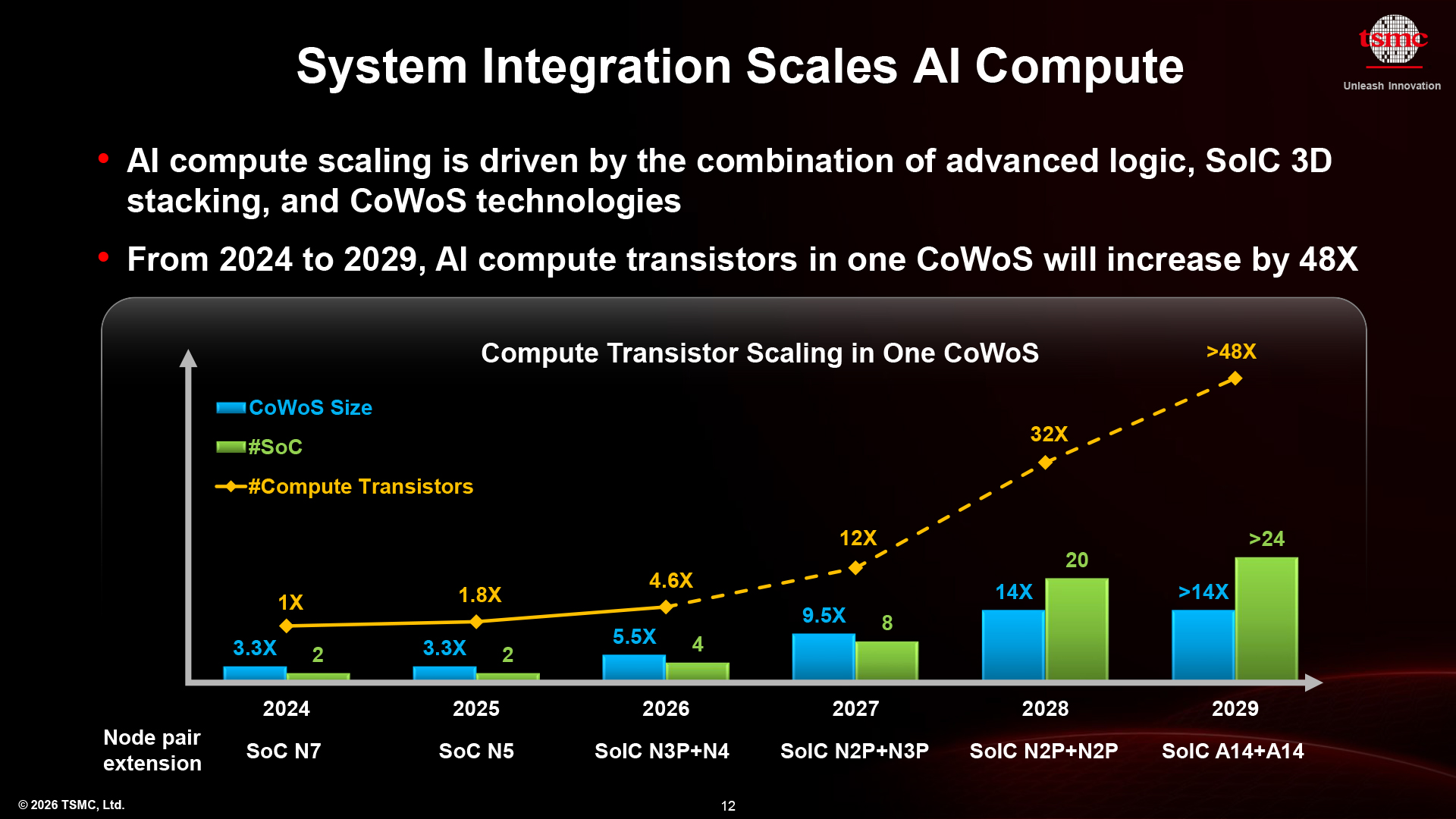
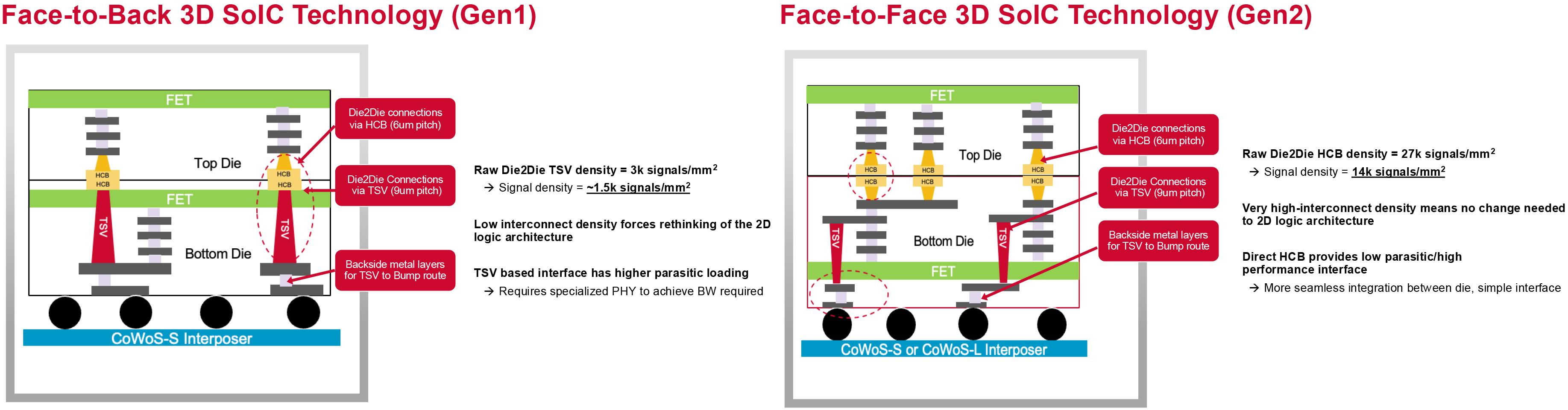
(Image credit: Getty Images / Anadolu) TSMC's chip-on-wafer-on-substrate ( CoWoS) packaging technology has become the de facto standard packaging method for advanced AI and HPC processors that use HBM memory, thanks to TSMC's aggressive development of the technology. Unlike lateral 2.5D CoWoS, TSMC's vertically integrated System on Integrated Chips (SoIC) technology with 3D interconnects has not been adopted as widely. However, now that the company has overcome the first generation's constraints, it will aggressively develop this technology in the coming years, as the company revealed at its recent North American Technology Symposium. Different kinds of stacking (Image credit: TSMC) Face-to-back stacking imposes fundamental limits because signals cannot travel directly between dies. Instead, they must cross multiple metal layers and pass across through silicon vias (TSVs) in the bottom die, which increases latency, power consumption, and routing complexity.…