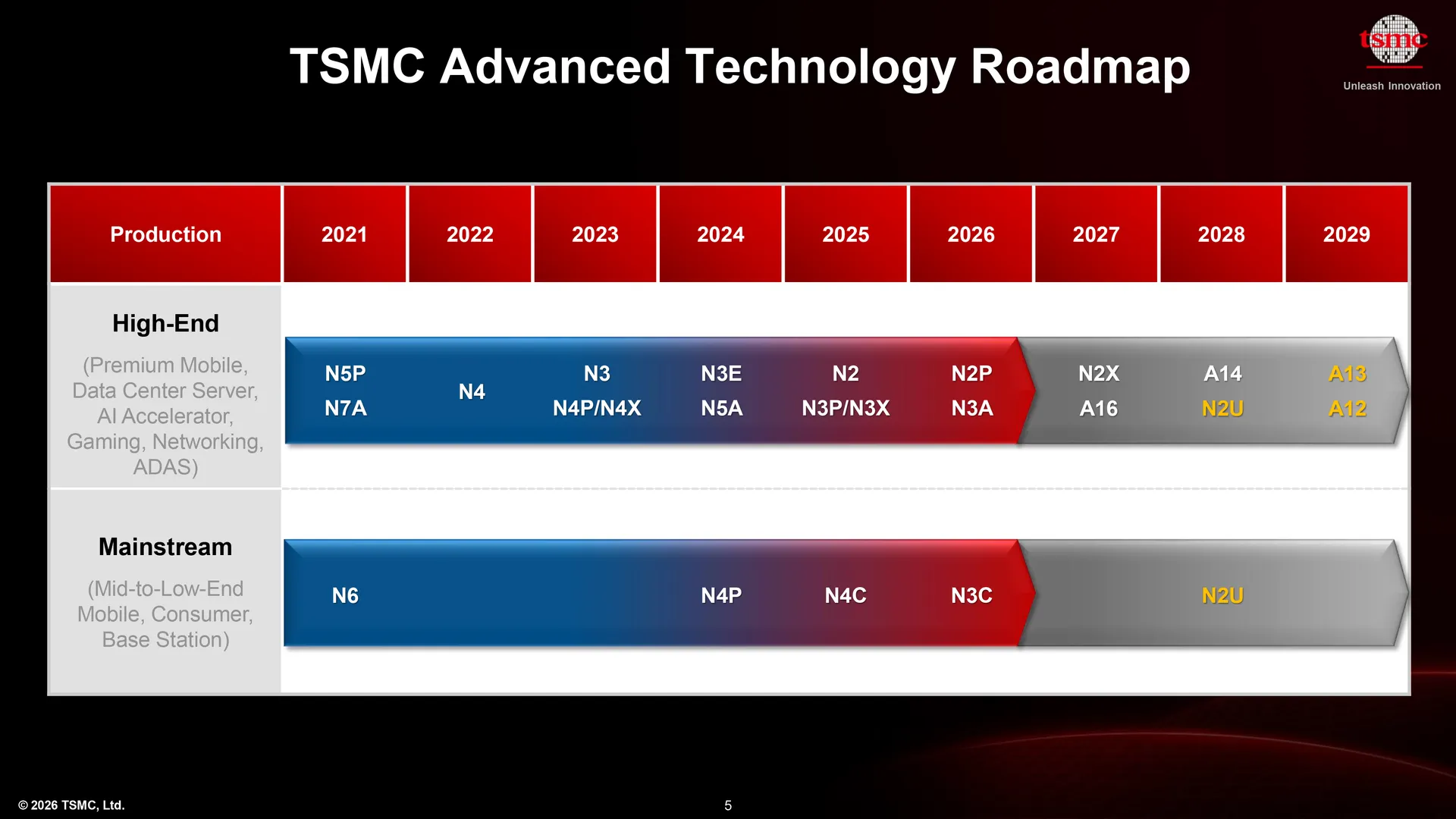
(Image credit: TSMC) TSMC revealed its general manufacturing technology roadmap through 2029 at its North American Technology Symposium 2026 on Wednesday. Among the key highlights the company presented were its 1.2nm and 1.3nm-class fabrication processes called A12 and A13, an unexpected extension of the N2 family named N2U, and the lack of plans to use High-NA EUV lithography for any nodes through 2029. Perhaps the most notable part of the technology-related announcement was firming the multi-faceted approach to new node development. Go deeper with TH Premium: Chipmaking Changing the rules of the game Historically the lion's share of TSMC's revenue originated from the smartphone industry, but more recently AI and HPC have outpaced handsets. This was clearly reflected in the company's plans, so TSMC's latest roadmap highlighted a deliberately bifurcated strategy that segments leading-edge nodes by end-market requirements rather than pursuing a one-size-fits-all approach.…